1. The thin film circuit process
Ultra-fine line circuit patterns are formed on the ceramic substrate by magnetron sputtering, pattern lithography, dry wet etching, and electroplating thickening.
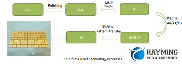
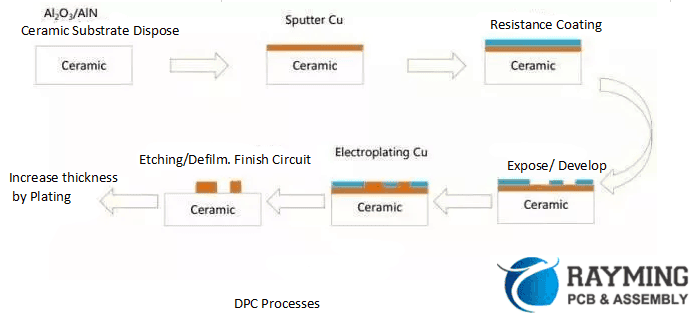
In the thin film process, based on the thin film circuit process, the surface of the ceramic is metallized by magnetron sputtering, and the thickness of the copper layer and the gold layer is greater than 10 micrometers by electroplating. That is, DPC (Direct Plate Copper).
2. Thick film circuit process
1), HTCC (High-Temperature Co-fired Ceramic)
2), LTCC (Low-Temperature Co-fired Ceramic)
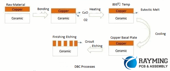
3), DBC (Direct Bonded Copper)
Related technologies in the production process of ceramic PCB substrates:
1), Drilling: The mechanically drilled holes are used to create the connecting pipes between the metal layers.
2), Plated through hole: After the copper line between the connection layers is drilled, the circuit between the layers is not turned on. Therefore, a conduction layer must be formed on the hole wall to connect the line. This process is generally referred to as “PTH” in the industry. Process, the main working procedures include 3 procedures: Desmear, Chemical copper and Electroplating Copper.
3), Dry film pressing: making a photosensitive layer of photosensitive etching.
4), Inner layer image transfer: use the exposure to transfer the image of the film to the board surface.
5), The outer layer exposure: After the attachment of the photosensitive film, the circuit board has been similar to the inner layer of the production process, again exposure, development. The main function of this photo film is to define the areas that need to be plated and do not need to be plated, and the area we cover is the area that does not need to be plated.
6), Magnetron sputtering: The energy and momentum exchange between the positive ions generated in the gas glow discharge process and the surface atoms of the target material are used to move the material from the source material to the substrate to realize the deposition of the film.
7), Etching – Formation of external lines: A technique in which materials are removed using chemical reactions or physical impacts. The functionality of the etch is reflected in the selective removal of specific graphics.
After the circuit is completed, the circuit board will be fed into the stripping, etching, and stripping lines. The main job is to completely strip the plating resist and expose the copper to be etched in the etching solution. Since the top of the wiring area has been protected by tin, an alkaline etching solution is used to etch copper, but since the wiring has been protected by tin, the wiring of the wiring area can be retained, so that the surface wiring of the overall wiring board is presented.

8), Anti-weld coating: The purpose of the ceramic circuit board is to carry the electronic component parts and achieve the purpose of connection. Therefore, after the circuit board circuit is completed, the area where the electronic parts are assembled must be defined, and the non-assembly area should be properly protected with the polymer material. Since the electronic components are assembled and soldered, the polymer material of the partial protective circuit board is called “solder paint”. Most of the current photosensitive solder resists are in the form of wet ink coating.
3. LAM technology process
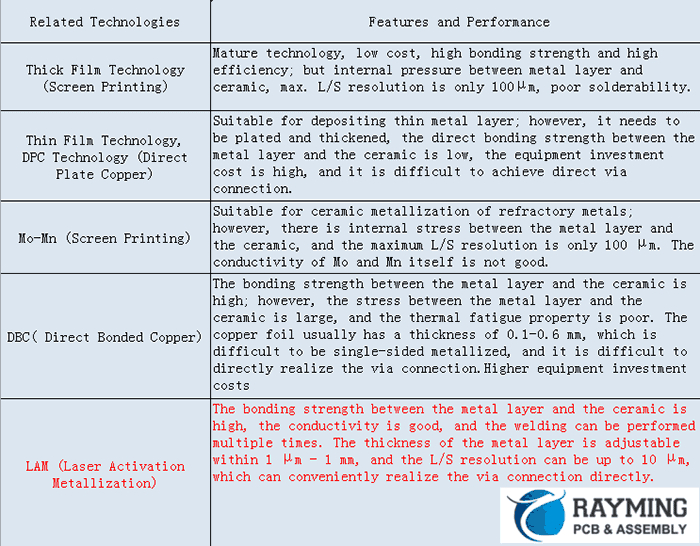
1), The bonding strength between the metal layer and the ceramic is high, the conductivity is good, and the welding can be performed multiple times. The thickness of the metal pcb layer can be adjusted within 1 μm-1 mm, and the L/S resolution can be up to 10 μm, which can conveniently realize the direct connection. .
2), LAM technology process production process:

3), LAM technology advantages:
A. Higher thermal conductivity: The thermal conductivity of the traditional aluminum-based circuit board MCPCB is 1 to 2 W/mk, the thermal conductivity of copper itself is 383.8 W/mK, but the thermal conductivity of the insulating layer is only about 1.0 W/mK. A little better can reach 1.8W/mK. The thermal conductivity of alumina ceramics is 20-35 W/mk, the thermal conductivity of aluminum nitride ceramics is 170-230 W/mk, the thermal conductivity of copper substrates is 2W/(m*K), and its thermal expansion coefficient Matching with commonly used LED chips, large Si-based chips can be directly mounted on the copper conductor circuit, eliminating the transition layer such as molybdenum sheets in the conventional module;
B. The metal film layer with stronger and lower resistance: the bonding strength between the metal layer and the ceramic substrate is high, and the maximum can reach 45 MPa (the strength of the ceramic piece larger than 1 mm thick); the conductivity of the metal layer is good, for example, The volume resistivity of the obtained copper is less than 2.5×10 −6 Ω·cm, and the heat is small when the current passes;
C. The solderability of the substrate is good, the use temperature is high: resistance to soldering, and the soldering can be repeated multiple times;
D. Good insulation: breakdown voltage up to 20KV/mm;
E. The thickness of the conductive layer can be arbitrarily customized within 1μm~1mm: any current can be designed according to the circuit module. The thicker the copper layer, the larger the current that can pass. The traditional DBC technology can only produce conductive layers with a thickness of 100μm ~ 600μm; when the traditional DBC technology is <100μm, the production temperature will be too high and will melt. When the thickness is >600μm, the copper layer will be too thick, and the copper will flow down, which will cause the edge of the product to be blurred. Our copper foil is covered, so the thickness is 1μm~1mm, and the precision is very accurate.
F. The high frequency loss is small, and the design and assembly of the high frequency circuit can be performed; the dielectric constant is small,
G. High-density assembly is possible, and the line/pitch (L/S) resolution can reach 20 μm, thereby realizing short, small, light and thinning of the device;
H. It does not contain organic components and is resistant to cosmic rays. It has high reliability in aerospace and long service life;
I. The copper layer does not contain an oxide layer and can be used for a long time in a reducing atmosphere;
J. Three-dimensional substrate, three-dimensional wiring


