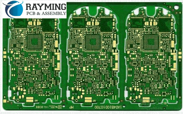
The HDI board, made for low-volume customers, is a compact board with a critical distinguishing feature of high wiring density compared to standard printed circuit boards. This difference between the two types of boards is mainly manifested in the given four aspects.
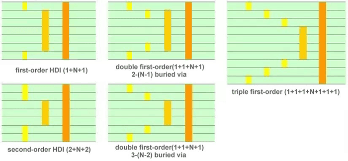
HDI PCB 1-step & 2-step, & 3-step
The initial step is pretty straightforward, with easily manageable procedures. However, the subsequent 2-step process becomes more intricate and presents several challenges, including counterpoint, perforation, and copper plating issues. Numerous two-step layouts exist, such as staggered positioning of each layer. This design allows connecting the adjacent coating to the intermediate layer via a wire equal to 2 first-order High-Density Interconnects (HDIs).
The second point is that 1st order vias intersect, resulting in a second-order effect achieved through superposition. Although the process is identical to first-order vias, several technical considerations require special attention, as discussed earlier.
The third step involves drilling from an outer coating to the 3rd coating or even the n-2 coating, which is a more challenging process than the previous steps due to the complexity of the hole. A similar approach can be analogized to the 3rd order.
Differences between HDI board & ordinary PCB
The commonly printed circuit board is made of fr-4, a combination of epoxy resin & electronic-grade glass fabric that is pressed together. In traditional HDI boards, the outer layer typically uses adhesive copper foil because the laser drilling cannot penetrate the glass fabric. Therefore, non-glass fiber adhesive copper foil is often used instead. However, with the development of laser ablation, it is now possible to penetrate 1180 fiberglass fabric, making the materials used in HDI no different from those used in standard PCBs.
1. HDI PCB – Smaller and Lighter
HDI PCBs have a core board that starts with a traditional dual-sided board and is then laminated with layers continuously. This method of layer accumulation is also known as BUM. When we compare it to conventional panels, these boards are “thin, light, small, and short,” providing several advantages.
HDI PCBs achieve interconnections between layers through conductive through-holes, buried vias, and blind vias. Unlike ordinary multilayer printed circuit boards, HDI boards (circuit boards) are made with massive no. of micro-bury holes.
Unlike standard PCBs drilled mechanically, HDI PCBs are prepared using lasers. This enables an increase in the number of layers & aspect ratio of the HDI PCB
2. High HDI Wiring Density

The high density of HDI PCBs is primarily evident in the density of holes, lines, and pads, as well as the thickness of interlayers.
HDI PCBs incorporate micro-through vias, including blind holes & another micro-via design. These designs exhibit two main features. Firstly, they involve hole-forming and micro-hole technology with diameters of at least 150 micrometers. Secondly, there are high demands on cost, production efficiency, and precise hole control. In multilayer PCBs, only pHTs are used, without tiny blind holes, as found in HDI PCBs.
HDI PCB manufacturing requires the improvement of line spacing and line width, which is reflected in increasingly strict requirements for wire defects & surface texture. Typically, the line width & line spacing do not exceed 76.2μm.
The thickness of pads on HDI PCBs is characterized by a density of more than 50 welded joints/square centimeter.
Thinning the dielectric substance is a critical aspect of HDI PCB manufacturing. This is mainly reflected in a trend toward reducing the density of the interlayer to 80 micrometers or below, with increasingly stringent requirements for thickness uniformity. This is particularly important for high-density plates & packaging substrates that require precise impedance matching.
3. HDI PCB with Better Electrical Properties
HDI PCBs not only enable more compact end-product layouts but also deliver more standards of performance & efficiency simultaneously.
HDI PCBs offer a higher interconnect density, resulting in improved signal strength & increased reliability compared to traditional PCBs. Moreover, HDI boards provide better protection against EMI, RFI, thermal conduction, and static discharge issues. HDI manufacturing also employs advanced DSP technology & a range of patented techniques, enabling the boards to handle a variety of load capacities and possess strong short-time load abilities.
4. HDI PCB has Strict Requirements for Buried and Plug Hole
Based on the information presented above, it is evident that HDI circuit boards outperform ordinary PCBs in terms of both volume & electrical performance. However, as with any high-end printed circuit board manufacturing process, HDI PCB manufacturing requires a higher threshold of expertise and involves more significant process complexities than the ordinary printed circuit board. Consequently, several issues require careful attention, particularly burying and plugging holes.
The most challenging aspect of HDI production is burying and plugging holes. Failure to adequately perform this step can lead to significant quality issues, such as uneven board borders, inconsistent dielectric thickness, pitted pads, and other related problems.
If the surface of the circuit board isn’t flat and there are depressions, it can result in a phenomenon known as “beaching.” This, in turn, can cause defects such as broken lines, line gaps, and other related issues.
Signal instability may occur as a result of fluctuating characteristic impedance caused by the uneven dielectric thickness.
When the pad surface is not even, it can result in poor packaging quality and loss of the component.
It is important to note that not all board factories can excel in producing HDI boards. However, Next printed circuit board has been dedicating its efforts to this field for over 15 years. Presently, RayPCB has developed its own comprehensive HDI system, with the entire manufacturing process being conducted in-house. The company has invested heavily in acquiring advanced equipment and adheres to stringent standards for Acceptable Quality, such as IPC2, which ensures high reliability. For instance, hole copper thickness is maintained at a minimum of 20μm.


