There has been some confusion regarding the differences between the CSP and BGA packages. Due to constant requests, we have decided to do more research and come up with an article that answers your questions.
In this article, we will be explaining from a neutral point what CSP and BGA packaging is. Furthermore, we will go on to explain the differences between the two, with respect to their features. If you need to widen your knowledge on this topic, get ready as we explain further.
What is CSP and BGA Packaging?
For some years now, many people understood the need to underfill flip chip devices. The traditional large BGA (ball grid array devices) are underfilled only on very rare occasions, probably when that specific device will be useful in some critical applications like flight computers. For some years now, there has been a debate regarding the importance of underfilling CSPs (chip scale packages).
Majority of package manufacturers try designing CSPs to prevent the underfill requirement. However, practically, the underfill CSP (chip scale package) will have a higher reliability in contrast to one not underfilled. Majority of manufacturers usually underfill the CSPs whenever the parts are utilized in applications for portable electronics which users usually drop.
Whenever the testing of the product reveals that there is a need to underfill a device, the next step you should take is determining the best underfill process. In this article, we will be discussing the differences when it comes to flip chip, the BGA and CSP device reviews and underfills where and when to make use of each process. Let’s continue as we do some csp bga comparison
Differences Between CSP Package and BGA Package
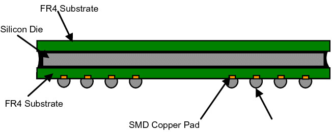
For newbies who have taken a BGA rework, so many people out there do not know the best way of distinguishing the CSP packages (chip scale packaging) from the BGA packages. Here we will clearly differentiate the difference between the two.
Ball Grid Array (BGA) Package
Due to the development of integrated circuit technology, the requirements for packaging integrated circuits are now more stringent. Why is this so? This is due to the relationship between the packaging technology and the product’s functionality. Whenever the IC’s frequency surpasses 100MHz, this traditional method for packaging may produce what is called the “CrossTalk” phenomenon.
Whenever the pin number is more than 208, this traditional method for packaging is difficult. Therefore, aside from the QFP method of packaging, the majority of high-pin count chips (like chip sets and graphics chips) are now making use of the BGA packaging technology.
Furthermore, for packages like CPUs, BGA has now become the most acceptable choice. For sure, there is a concern for many people regarding the BGA rework packages.
Categories of BGA Packaging Technology
Plastic BGA (PBGA)
This is a multi-layer board, which is made up of two to four layers of different materials. Note that, among the Intel series central processing units, the Pentium IV, III, and II processors make use of this package.
CeramicBGA Substrate (CBGA): The electrical connection, which is found in-between the ceramic substrate and the chop is mounted via the Flip Chip (FC). Note that, among the Intel series central processing units, the Pentium Pro, Pentium II, and I processors make use of this package.
Flip Chip BGA (FCBGA): This is a multilayer and rigid substrate
Tape BGA substrate (TBGA): This substrate refers to a soft strip-shaped PCB circuit board of 1-2 layers
Carity Down PBGA (CDPBGA): This substrate has to do with the bare chip area, which is also referred to as the cavity area having a low depression at the package’s center.
What are the Features of the BGA Package?
- Though there is an increase in the input output pins, there is a much larger distance in-between the pins compared to the QFP packing that aids yield improvement.
- Though there is an increase in BGA consumption, since controllable chip welding is usually used, there can be an improvement in electrothermal performance and thermal expansion.
- There is a small delay in signal transmission, while there is great improvement in adaptive frequency.
- You can make use of co-planar welding for assembly. This helps in improving the reliability greatly
CSP Package (Chip Size)
With the increase in demand for lightweight and personalized electronic products globally, their packaging technology has seen great advancements to the Chip Size Package (CSP). This reduces the chip’s package size, making sure that the IC has over 1.2 times of the chip’s side length, and the area of the integrated circuit (IC) is a maximum of 1.4 times larger compared to the die.


