Printed circuit boards (PCBs) are essential components in most electronic devices today. However, they are also very delicate and can be easily damaged during shipping if not packaged properly. Choosing the right packaging materials and methods is crucial to ensuring your PCBs arrive at their destination safely.
In this comprehensive guide, we will look at everything you need to know about PCB packaging and shipping, including:
- Benefits of proper PCB packaging
- Common PCB packaging materials
- PCB packaging methods
- PCB shipping considerations
- Packaging for domestic vs international shipping
- Packing and labeling requirements
- Best practices for preventing shipping damage
Properly packaging your PCBs takes time and effort but is well worth it to avoid costly damages during transit. By following the recommendations in this guide, you can have peace of mind knowing your PCB shipment will make it to its destination intact and ready for use.
Benefits of Proper PCB Packaging
Packaging may seem like an afterthought, but it is one of the most critical steps in ensuring your PCBs arrive safely. Investing in proper packaging materials and techniques can provide the following benefits:
Prevents Damage: Good packaging protects your PCBs from the inevitable shocks and vibrations of shipping. Without adequate cushioning and immobilization inside the package, PCBs can be cracked, bent, or scratched.
Reduces Repairs/Replacements: When PCBs arrive damaged, you face expensive rework, repairs, or complete replacements. Proper packaging greatly reduces damage rates.
Saves Money: Damaged PCBs and subsequent troubleshooting/repairs cost money. The upfront investment in quality packaging pays for itself by preventing these expensive issues.
Maintains Quality: Any damage to a PCB risks quality defects or performance issues in the final product. Good packaging maintains the pristine condition of your boards.
Improves Customer Satisfaction: Your customers expect boards to arrive intact and ready for their own manufacturing processes. Packaging helps ensure you meet their expectations.
Complies with Regulations: Certain industries have packaging regulations you must comply with. Aerospace and defense, for example, have strict requirements.
The bottom line is that effective PCB packaging is not just about materials, but about protecting product quality, reducing costs, and improving customer satisfaction.
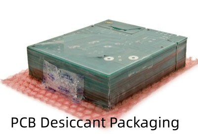
Common PCB Packaging Materials
PCBs are packed with great care because even the smallest crack or chip can render a board non-functional. There are a variety of packaging materials designed to keep PCBs safe in transport:
Cushioning Materials
Cushioning materials protect PCBs from physical impact and vibration. Recommended options include:
- Bubble wrap – The air bubbles provide excellent cushioning against shocks. Bubble plastic comes in different bubble sizes. Use small bubbles for delicate PCBs.
- Foam sheets – Foam is available in anti-static varieties for protecting sensitive electronics. Closed-cell foams provide the best shock absorption.
- Air pillows – These air-filled cushions mold around PCBs and prevent movement inside boxes. They come in anti-static materials.
- Paper cushioning – Recycled paper formed into accordion sheets or crumpled paper makes an eco-friendly cushioning option.
Immobilization Materials
Immobilizing materials prevent PCBs from shifting inside the packaging. Suitable solutions include:
- Cardboard partitions – Die-cut cardboard pieces physically separate PCBs and hold them in place.
- Plastic trays – PCBs can be inserted into plastic tray molds to keep them immobilized.
- Foam inserts – CNC-cut foam fits around PCBs like a glove, keeping them snugly in place.
- Tape – Specialty tapes can be used to adhere PCBs to interior packaging surfaces.
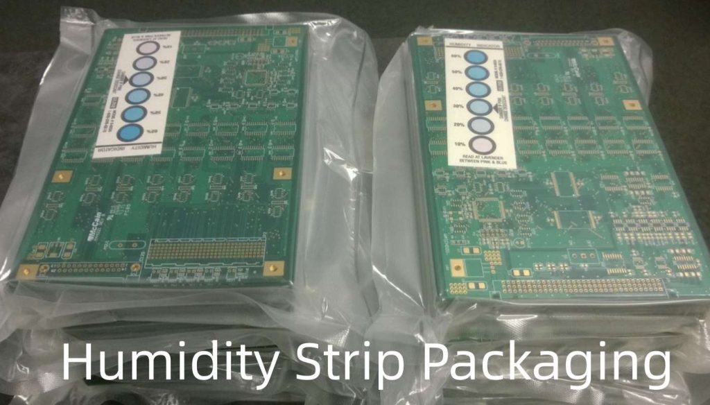
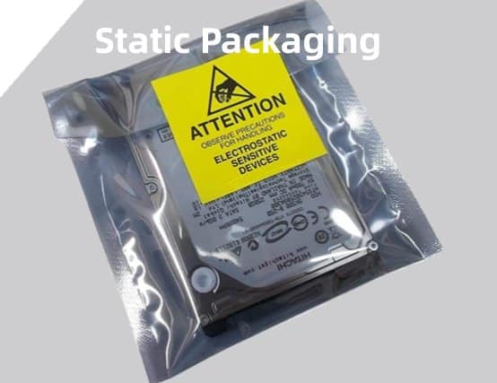
Static Protection Materials
Static-sensitive PCBs need antistatic packaging materials, including:
- Antistatic bags – Metallized shielding dissipates static charge away from the PCB inside.
- Antistatic foam – Dissipative or conductive foam prevents static buildup.
- Metalized bubble wrap – Metallized top layer renders bubble wrap antistatic.
- ** Carbon-loaded plastic** – Plastic discharge sheets prevent static accumulation during transport.
Cushioning Materials Comparison
| Material | Shock Protection | Vibration Damping | Static Protection | Cost | Environmental Impact |
|---|---|---|---|---|---|
| Bubble Wrap | Excellent | Fair | Only if metallized film | Low | Recyclable |
| Foam | Good | Excellent | If anti-static foam used | Medium | Recyclable |
| Air Pillows | Very Good | Good | If anti-static material used | Low | Not biodegradable |
| Paper Cushioning | Good | Fair | No | Very Low | Biodegradable |
PCB Packaging Methods
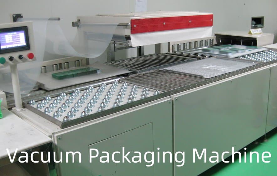
Packaging best practices involve using multiple protective materials strategically to create a secure package:
1. Cushion Base
Start by lining the bottom of your box/container with cushioning material – bubble wrap, foam, or paper. The cushion base will absorb impacts from the bottom during shipping.
2. Static Shielding
For static-sensitive PCBs, line cushioning with a static dissipating material like metallized bubble wrap or antistatic foam. This shields PCBs from static inside the package.
3. Immobilization
Next, place PCBs inside die-cut cardboard, plastic trays, or foam cutouts. This immobilizes the boards and prevents shifting/collisions.
4. Cushion Top
Finish with another cushion layer on top to protect PCBs from crushing or dropping impacts.
5. Secure Container
Place the protected PCBs inside a rigid outer box, tube or other container. Tape securely to prevent accidental opening.
6. Labeling
The outer container should be clearly labeled as fragile and contain shipping/handling instructions. Apply all necessary shipping labels.
This layered approach minimizes motion and isolates PCBs from vibration, shock, and abrasion during shipping. Adjust packaging for PCB size, quantity and shipment mode.
PCB Shipping Considerations
To choose the optimal PCB delivery method, consider these factors:
Delivery Timeframe
How quickly do the PCBs need to arrive at their destination? Timeframes range from next day air to ocean freight that takes weeks.
Quantity to be Shipped
The quantity of PCBs being shipped impacts the packaging and shipping mode choices. A few boards can go by air but high volumes require ocean/ground.
Shipping Distances
The distance PCBs need to travel affects transit time and cost considerations. Overseas shipments adds complexity.
Risk Tolerance
Some applications can accept a higher risk of damage (i.e. prototypes) vs others with zero damage tolerance (medical devices).
Security Requirements
Some PCBs contain sensitive IP/data necessitating security measures during transit.
Cost Sensitivity
Faster, lower-risk shipping methods cost more than slower cargo transport. Budget determines acceptable shipping costs.
Sustainability Goals
Companies increasingly prioritize environmental footprint. Greener transport options are slower but reduce emissions.
Consider all these factors when selecting PCB delivery methods, carriers and service levels.
Domestic Shipping Methods
For domestic PCB transport within your country, common shipping options include:
Ground Transport
- Truck – Reliable option for cost-effectively reaching domestic destinations within days. Higher risk of shocks/vibrations.
- Rail – Cargo trains offer secure transport for large PCB quantities with minimal handling. Slower transit times.
Air Transport
- Air Freight – Quick way to ship small, high-value PCBs domestically. Costlier but lower damage risk.
- Next Day/Overnight Air – Guaranteed next day delivery for urgent shipments. Most expensive option.
Postal Systems
- Express Mail – Fast public postal networks like USPS Express or Royal Mail Special Delivery. Low cost for small packages.
- Couriers – Private carriers like FedEx, UPS, DHL. Offer express options and package tracking.
Ground and air methods both have pros and cons. Assess speed needs, cost and risk tolerance for each shipment.
International Shipping Methods
For overseas PCB transport, main options are:
Air Freight
- Passenger Planes – Available space in passenger aircraft cargo holds. Fast transit but high cost.
- Cargo Planes – Only freight pallets/containers aboard these planes. Moderate speed and expense.
- Charter Planes – Renting an entire cargo plane. Very fast but extremely costly.
Air cargo is the quickest way to move PCBs overseas although costs accrue rapidly for large volumes.
Ocean Freight
- LCL – Less than container load. PCBs consolidated with other cargo in a shared container. Slow but more affordable.
- FCL – Full container load. A dedicated container for your PCB shipment. Cost-effective for large quantities.
- Courier – International couriers use both air and sea methods. Offer door-to-door services.
Sea freight takes weeks but offers low costs for heavy PCB loads. Air and sea can be combined to balance speed and affordability.
Packing and Labeling Requirements
Follow standard packing protocols to facilitate safe PCB transport:
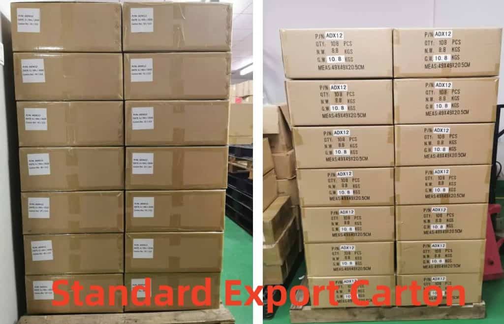
Use Strong Outer Boxes
Sturdy corrugated cardboard boxes properly sized for contents. No more than 75% full.
Cushion Box Interior
Layers of shock/vibration absorbing materials immobilizing and protecting PCBs.
Seal Securely
Reinforced tape on opening seams and closure prevents accidental opening.
Fragile Labels
“Fragile” labeling alerts handlers to gently transport the PCB package.
Arrow Direction Indicators
Indicates correct upright box orientation during shipping and storage.
Full Address Labels
Clear origin/destination address labels for accurate delivery. Include contact info.
Customs Paperwork (international)
Required commercial paperwork like commercial invoices, packing lists etc.
Compliance Markings
Any required government/regulatory compliance labeling like for hazardous goods.
Center of Gravity/Lift Indicators
Marks center of gravity and where to safely lift heavy loads.
Proper labeling maximizes safe handling and ensures the correct delivery of PCB shipments.
Preventing Shipping Damage
Despite best packaging efforts, PCBs still risk damage during shipping if proper precautions aren’t taken:
Packing Method
- Use only ESD-safe packaging materials and eliminate static hazards.
- Immobilize PCBs fully to prevent shifting/banging in transit.
- Don’t overpack boxes as it can lead to crushing of contents.
- Test package with shock/vibration simulations before shipping.
Handling & Storage
- Label packages clearly as fragile – include any orientation needs.
- Ensure carriers understand any special handling requirements.
- Stipulate covered, temperature-controlled storage if needed.
- Discourage unnecessary handling like transloading goods multiple times.
Shipping Mode
- Match your chosen mode/carrier to the PCB shipment characteristics and risk profile.
- Be aware of environmental hazards like moisture and avoid freight staging delays.
- Where possible, use direct routings to minimize handling exposure.
Security
- Use tamper-evident seals to prevent undetected access to packages.
- Ship high-value or sensitive PCBs using secure logistic methods.
- Require signature confirmations at delivery to assure custody.
Quality Reviews
- Inspect PCBs upon unpacking to quickly identify any shipping damage.
- Provide feedback to carriers regarding mishandled packages.
- Continuously evaluate and identify ways to improve your packaging.
Attention during packing, shipment planning, and quality oversight helps mitigate damage risks and ensures effective PCB delivery.
PCB Packaging FQA
Here are answers to some frequently asked questions about PCB packaging:
Are antistatic bags essential for shipping PCBs?
Antistatic shielding is strongly recommended whenever shipping electronics like PCBs to prevent static discharge damage. The conductive shielding of antistatic bags dissipates any accumulated static charge away from sensitive components. Without proper static mitigation, even low levels of charge built up through routine handling and transport can destroy or degrade microelectronics. Antistatic bags are an inexpensive way to add this important protection layer.
How should I package a large panel PCB for shipping?
For oversized PCB panels, the goal is securing the board flat to avoid bending while providing adequate padding from physical impacts. One method is to place the panel between two rigid sheets – acrylic, polycarbonate or stiffness-enhancing cardboard. Use several spacers or standoff screws between the sheets to prevent direct contact/abrasion against the PCB surfaces. Then wrap this assembly in shock-absorbing foam inside a rigid outer case. The case keeps the PCB immobilized and protected.
What labeling identification should be on a PCB package?
PCB packages should have clear exterior labeling that informs handlers how to properly transport and deliver the product. This includes “Fragile” markings, any required orientation arrows, shipping address, and contact info. For mixed PCB shipments, individual boxes should have unique package IDs and contents details so the recipient can confirm what’s inside. Useful identifiers include PCB part numbers, version numbers, manufacturing dates and tracking codes.
Does ESD packaging prevent all static damage during shipping?
While ESD packaging like antistatic bags and foam help safeguard electronics from electrostatic discharge events, they cannot guarantee 100% protection from static damage, especially for highly sensitive components. Such packaging provides shielding under typical transport conditions but does not fully isolate contents from any and all possible ESD risks like a Faraday cage. Additional diligence around packing/unpacking, avoiding contact with highly insulative materials, humidity control and grounding is still needed when handling especially vulnerable PCBs and ICs.
What are some eco-friendly solutions for packing PCBs?
Green packaging options for PCB transport include paper cushioning instead of plastic foams, biodegradable corn starch-based packing peanuts, recycled cardboard boxes, and avoiding single-use plastics. However, effectiveness should not be sacrificed – eco-friendly materials that fail to adequately protect PCBs help no one. A balanced approach considers environmental impact alongside product protection. Some examples are combining recycled paper padding with reusable plastic trays for immobilization, or 100% compostable PLA air pillows used with recyclable cardboard partitions.
Conclusion
The safe delivery of PCBs from manufacturer to end-user relies heavily on robust, well-engineered packaging solutions. Attention must be given to cushioning, immobilizing and shielding PCBs from the unavoidable stresses of shipping. Matching packaging methods to the unique characteristics of each PCB shipment requires an understanding of available materials, regulations, transport modes and potential risks. With proper planning, preparation and quality control, companies can have confidence their PCB investment will arrive intact and functioning, ready for installation and use. Effective packaging is an integral part of the overall PCB supply chain.


