A PCB trace width is simply a parameter defining the distance covered across a circuit board’s trace. Some other well-known parameters here include trace thickness and spacing. Four major factors influence the PCB trace width. These include:
- The desired length of the trace
- The spacing required between these traces
- The size of the board’s conductive layer
- The capacity of the trace necessary to carry current
PCB Trace Width Calculator: What does this mean?
No matter the type of industry you work in, every day you may use a printed circuit board. These devices are very important to how electronics function. Also, they connect and offer mechanical support to electrical components. This is to ensure that they operate properly.
When utilizing Printed Circuit Boards to sustain computers, lighting technology, or medical equipment, they must operate with the right trace width. Using a circuit calculator, you will be sure of the safety of your printed circuit board. They will also stay functional all the time.
The use of the IPC-2221 standard is the major factor in the derivation of a PCB trace width calculator. This standard helps in calculating the conductive track width of a printed circuit board (PCB). It is advisable that you design the PCB traces in order to bear the highest current load even before they start malfunctioning.
The determination of the copper width calculation, at a specific thickness, is necessary. This helps in allowing the transfer or movement of a particular current value. In addition, the copper thickness and width need to be enough to help maintain the rise in temperature at levels below the input.
How to get Trace Width Making Use of a PCB Trace Width Calculator

This calculator needs the imputation of some values to know the trace’s desired width. The representation of this width is in mils & deals with the utilization of some values. These include:
- The conductive layer’s area, which is usually in mils square
- The trace’s thickness, which is in ounces/sq ft
What differentiates the External vs. Internal PCB Trace Width Calculators?
Internal PCB trace width calculators are tools that determine the required width of an internal trace. The determination of this internal trace width is to help carry a specific current amount.
External PCB trace width calculators are similar tools, which tell an external trace’s width. The result of the trace width also, is useful for the transfer of the current of a particular amount.
Consequently, the difference seen between the external and internal traces has to do with their location. This location relates to the substrate of the board.
Also read about SMT Engineer
Why is Using a PCB Trace Width Calculator Important?
During the production of PCBs, you will discover that the limitations of current-carry are a major constraint.
You may trace a PCB successfully and then later discover that it will not be able to carry the needed amount of current effectively. Consequently, the printed circuit board’s intended application experiences a setback. This is due to the inadequate current capacity.
Making use of your PCB trace width calculator ensures the conductance of the right current value. Using this circuit calculator, you may utilize the highest current rating you desire to know the width of your trace.
In addition, you may influence the rise in temperature which your PCB records. This is possible by making use of your PCB trace width calculator.
More Facts about the PCB Trace Width Calculator
Engineers often utilize the PCB trace width calculator in the fabrication process of a PCB. This tool helps to detect a lot of things in a circuit board. Before fabricating a PCB, you need to understand how the element works. Other important things you need to know about this tool are discussed here.
It is very important you detect the conductive layer’s area. You can use some constant values to determine this area. The IPC-2221 can help you to derive the constant values which are b, k, and c. These values vary depending on the location of the trace. The location of the trace can either be internal or external. The values of these constants are requirements for conductive material.
Detecting the temperature of the trace helps to know your PCB’s thermal performance. This plays a significant role in knowing the important properties of a PCB. You can sum the highest desired increase in the temperature. This will help you to get the overall temperature trace. The values of the temperature are in °C.
The PCB trace width calculator has a mil. This mil plays a vital role. In the PCB world, mil is a terminology. It is frequently used when talking about the thickness of the circuit board layer. For instance, you can express copper thickness in ounces and as well as convert it to mils.
You don’t need the trace width to determine dissipated power and the voltage decrease. However, you need to understand the resistance value and the value of maximum current. This will help to tell or reveal the loss of power and voltage drop.
Use the overall resistance value and the maximum current value to get voltage drop. Multiply the maximum current value’s square and the value of resistance to get the power loss. All of these things should be taken into consideration. This will help calculate the voltage drop and the dissipated power.
What Does It Mean To Experience a Rise In Temperature When Calculating The PCB Trace Width?
When there is a flow of current via a conductive trace, there is a generation of heat. This is a result of the resistance it gives to the conductor’s flow of current.
The increase in temperature defines the generation of heat. We refer to this as the rise in temperature. Also, you may determine how much rise in temperature your PCB will be able to sustain. This is possible by making use of a PCB trace width calculator.
When you provide PCB trace widths that are wider, you will be able to reduce the buildup of heat. This then results in a rise in temperature.
For many printed circuit boards, a temperature rise of 10 degrees is safe. Otherwise, you can fabricate boards to withstand a higher value in temperature rise. Also, you will find the application’s environment. This will help influence the board’s overall temperature.
Can You Extract Other Measurements By Using the PCB Trace Width Calculator?
PCB trace width calculators allow you to be able to establish different PCB measures. You can include additional input parameters. These include the trace’s length and the temperature for operation. This helps to extract additional measurements. Due to this, you can determine the measures below.
- The power dissipated along the trace
- A drop in voltage across the pcb trace
- The trace’s resistance value
- The trace’s rise in temperature
Can Board Spokes Be Subject to Trace Width Calculation?
Now PCB wagon wheels or spokes are features of the board design. These features help in simplifying the process of soldering for any ground plane.
They look like traces. However, they have a short length and are usually inserted inside the plane. Whenever you are making use of a trace width calculator, people hardly consider the spoke. This is because not all printed circuit boards have them.
It is however compulsory to ensure that spokes have a reduced width compared to actual traces. This is done without basing it on calculations.
Can we regard the Cross sectional Area of the Conductive Layer as an Important Parameter in Calculating a PCB Trace Width?
Yes, this is a very important parameter. The conductive layer’s cross sectional area is a very significant input when ascertaining the PCB trace width calculator.
This area in question is given in mils squared. This area is useful as the numerator for the calculation of the division of the trace width.
Determining the conductive layer’s cross sectional area requires some parameters. These parameters are highlighted below.
- The maximum rise in temperature permitted which is in °C
- Three constants c, b, and k are different when there are external or internal traces.
- The maximum current permitted which is calculated in Amperes
Can the PCB Trace Width Calculator Detect the Trace Resistance?
To get your trace’s resistance value, you can make use of a PCB trace width calculator. PCB engineers have to calculate the trace width to know the value of resistance. The below parameters is needed for the trace width:
- The trace length in centimeters
- The overall or total temperature of trace
- The trace thickness measured in ounces/ sq ft
- The conductive layer’s cross sectional area
- The conductive material’s resistivity value
Calculating the current-carrying capacity
Calculating the current of the trace width of a PCB is very important. You can achieve this by using different methods. There is a method that utilizes a circuit calculator that determines the current of a PCB trace. Another method utilizes the PCB width calculator.
It is very important to detect the current carrying capacity of the board. You need it when you have to evaluate the application limit of the board. Knowing the current limitations of the PCB trace width is important. It will help you to prevent exposing the circuit boards to possible damaging use.
What Determines Maximum Current-carrying Capacity?
The cross sectional area of the trace often determines the current carrying capacity. The temperature rise is also important. The trace’s cross sectional area is directly proportional to the copper thickness. The same goes for the trace width.
To get the maximum carrying capacity, you need a simple formula. Some practical cases are not easy to calculate. This is due to the rise in temperature and cross sectional area. Other things also determine the current carrying capacity of the trace. These things may include vias, components, and pads.
Traces that have many pads will function more than ordinary traces. Engineers place circuit boards on some trace between pads. This happens when there is abundant solder paste on pins or components. When this occurs, it results in an increased cross sectional area. Increasing the trace width provides a solution to this problem.
When you can’t widen a trace, you can apply a solder mask on traces. The surface Mount Technology procedure needs solder paste. Trace width will increase after reflow soldering. This will help the current carrying-capacity to also rise.
One can get the trace current carrying capacity of a PCB using a formula. This application is ideal for straightforward trace calculation. It is important to consider contaminant pollution in the fabrication of a PCB. Pollution can result in the breaking down of some traces. There must be a security factor to prevent the issue of overloading.
Engineers also need to pay special attention to turning traces. If there is an acute angle in a trace, there will be a non-smooth transfer. This can have an effect on small traces or current with a large width. However, when the current-carrying capacity is low, there might be issues.
What is the difference between external and internal trace widths?
People wonder how to differentiate between the external and internal traces. You can know the differences through their location. Internal traces are PCB’s inner layers while external traces are on the outer surfaces of the PCB.
You will realize that the internal traces are greater than the external traces. It is vital you note that the parameters ‘values for both internal and external traces may vary. These parameters are the conductive material’s constant values and cross sectional area.
With time, you will notice that this is due to the various thermal requirements and construction differences. The major function of this PCB trace width calculator is taking control of the rise in temperature. When you expose external traces, they allow heat to discharge partly via convection.
Layers that are not conductive cover internal layers which lead to the accumulation of heat. To increase heat dispersion’s surface area, the internal traces have to be bigger.
Are there other ways to detect the amount of current a PCB can carry?
There is no doubt that the PCB trace width calculator helps to detect the current capacity a trace can take. However, you need to understand some features of the board. These things can help to add more to the carrying capacity of the trace.
For example, the vias system and the pads can affect the amount of current that can move via a trace. In a PCB, conductive vias provide alternative ways for the flow of current. This allows the production of narrower traces.
Due to this, there can be a huge circuit density that boosts the performance capabilities of the board. Another factor that can cause current flow of trace is the amount of attached parts onboard. You will realize that some electronic components feature great power demands. These components come with exceptional thermal dissipations.
With this explanation, one can easily say that a PCB trace width calculator is very important. In the fabrication of a printed circuit board, engineers need this tool. It is a very important tool that cannot be overlooked in the PCB industry. It has got a lot of benefits and has also made the fabrication of PCB an easy process. PCB manufacturers are very much familiar with the PCB trace width calculator.
Formulas Associated with PCB Trace Width Calculator
For a PCB trace width calculator, you have to understand some basic formulas. These formulas will help understand your calculator better.
Trace Temperature
This is an important element that helps you get your trace width. You can calculate the trace temperature by summing T RISE and T AMB. You only need three total parameters to calculate trace temperature.
- T TEMP is Trace temperature
- The T AMB is ambient temperature
- T RISE is the maximum rise of the desired temperature
Power Dissipation Calculator
When an electronic device produces heat then there is power dissipation. This can lead to loss or waste of energy. To get the power dissipation, you need the maximum current and resistance value. Therefore, P Loss= R * I2
- Power loss = P Loss
- Resistance = R
- Maximum current = I
The maximum current uses ohms for its measurement while resistance uses watts.
Max Current
To get the maximum current, use A= (T X W X 1.378 [mils/oz/ ft2)
- [Mils2] is the trace thickness
- A is the cross section area
- [oz/ft2] W is the width of the trace
After solving this equation you can now detect the maximum current. Use this IMAX = Ac x (k x T RISEb) to achieve this.
The parameters mean
- Maximum current= [mils] IMAX
- Maximum rise of desired temperature= [A] TRISE
- Constants =b, k, and c
Voltage Drop Calculation
When calculating the voltage drop of a PCB, you need trace resistance and maximum current. The voltage drop measures the reduction of electrical potential in an electrical circuit.
Voltage drop= Maximum current * trace resistance.
Resistance Calculation
You will have to convert the cross-section area when you want to calculate the PCB’s trace resistance. Resistance= (1 + a * (T TEMP – 25 degree Celsius) (p * L / A).
- Trace thickness= T
- The trace temperature = [1/ °C] T TEMP
- Trace width= [oz/ft2]
- Resistivity temperature coefficient =[cm] α
- Trace resistance= [mils] R
- Trace length= [Ω · cm] L
Frequently Asked Questions
It could be a difficult and confusing process when you are calculating the trace width. This holds especially for those new to using a trace width calculator. Some questions have been bothering you with respect to this calculator. It may be with the results or formula, and you may find an answer to them here.
Is there a limit to the current that this calculator can use in calculating the width? Of course, this has to do with whichever formula you are using. This tool can calculate trace width of about 35 amps, 400 mils, and copper falling within 0.5 – 3 ounces /sq ft and an increase in temperature falling in the range of 10 to 100 degrees Celsius. This calculator extrapolates the data anytime you use it outside any of these ranges.
What is the mils unit of measurement? The word “Mil” is from a Latin term called “mille,” which means “thousand.” One mil is an inch divided into a thousand places.
Why is it that the calculator reveals the width of the internal trace higher than that of the external trace? High heat transfer is usually associated with external trace layers. Internal layers, on the other hand, don’t also conduct heat. This means that internal traces will be able to store more heat.
In this context, what do we mean by temperature rise? A rise in temperature has to do with the difference between the maximum operating temperature of your PCB regarded as safe, and its normal operating temperature.
While using this calculator, I put in a current requirement of 65 amps, and it brought back an incorrect track width. So what are its limits? This tool works with an original graph that only covers about 35 amps. It also works with a trace width of 0.4 inches. Also, it only deals with a rise in temperature from 10 – 100 degrees centigrade. Lastly, it works with a copper of about 0.5 – 3 ounces for every square foot. Anything outside these ranges will lead to an extrapolation of these formulas.
Conclusion
As already mentioned, printed circuit boards serve as backbones for many electronic products. By now, we hope you have been enlightened on why you need to establish the trace width of your printed circuit board. This helps to prevent and safeguard it from any destruction. When you establish the trace width, you will be able to know the amount of current. Lastly, make sure you abide by all the standards set. These help in creating a good PCB.
Trace width of a Printed Circuit Board (PCB) is a basic yet very crucial parameter which needs to be defined while designing a PCB. Calculation of trace width is important for both power and signal boards. This parameter defines the current carrying capacity of a PCB. Before going into the details of trace width, it is important to look at the factors which limit the flow of current through a conductor. Any conductor with a specific (cross sectional) area ‘A’ carrying the electrical current ‘I’ offers an electrical resistance of ‘R’ towards the flow of current. The electrical resistance results in the loss of electrical energy into the heat dissipation which depends on the square of the current flowing through the conductor (hence these losses are known as I2R losses). With the rising current, the heat dissipation also increases and beyond a certain point excessive heat results in failure of the current carrying conductor. To reduce the heat dissipation (I2R losses) in the conductor the resistance needs to be decreased. Electrical resistance of a conductor is inversely proportional to the area ‘A’ and directly proportional to the length ‘L’ of the conductor.
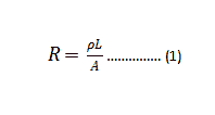
‘ρ’ is the electrical resistivity of the conductor material under consideration. For copper, the resistivity is 1.7×10⁻⁸ (ohm-m). If the length needs to remain constant, area can be increased to reduce the electrical resistance. Or in other words, increasing the area of the conductor increases its current carrying capacity (by reducing the heat losses or I2R losses).
This methodology of increasing current carrying capacity through increase in area now can be extended towards PCBs as well. ‘Traces’ on a PCB (sometimes also referred to as tracks) are the copper electrical connections responsible for carrying the electrical current. Due to the two-dimensional nature of a PCB circuit, the ‘width’ of traces is used to define the maximum amperage of a PCB board rather than the cross-sectional area (as height becomes a constant after choosing a thickness of copper). The formula for calculating the trace width is derived from following mathematical expression below (published in IPC-2221 standard):
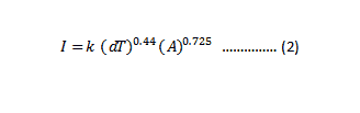
Where,
I= Maximum current (A)
dT= increase in temperature above ambient (°C)
A= cross-sectional area (mils2)
‘k’ is constant which depend on the position of traces on the board
k (for internal traces) = 0.024
k (for external traces) = 0.048
Reason for different values of k is that the traces on the outer side of the PCB have a better chance of heat dissipation through the process of convection as compared to the internal layers. As a result of that, heat starts to accumulate on the internal layers. Higher value of ‘k’ for the internal layer means wider trace width which helps dissipate the accumulated heat. However, if the circuit is placed inside complete vacuum, the outer layers cannot lose heat through the process of convection. So, while designing PCBs in a vacuum, same value of ‘k’ needs to be chosen for internal and external layers i.e. 0.024.
The exponents of ‘dT’ and ‘A’ are a result of physical constants of copper such as resistivity of copper and temperature coefficient of copper. Area of trace (mil2) can be calculated by rearranging (2) as shown below:

With a chosen thickness ‘T’ (mils), the trace width ‘w’ (mils) can be calculated:
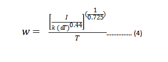
Figure below depicts the (for a contact thickness of 1oz or 35 um) current capacity against the calculated trace width for different changes in temperature from ambient.

Although the formula in the equation (4) does not have a mathematical limit, its accuracy keeps decreasing with higher values of current and trace width. For values of current higher than 35 A for outer traces 17.5A for internal traces or trace width higher than 400 mil, this formula will result in significant error value. Additionally, the mathematical formula to calculate the trace width does not keep into account some other factors such as count of electronic components, vias and pads in the circuit. And finally, factors like dust are also taken into account in large scale production of PCBs. This mathematical formula also assumes that the components do not cause any hindrance in heat dissipation. That’s why an additional buffer is added to the calculated value to avoid complexities arising from external factors.
It is also important to maintain proper spacing between the traces to avoid any transient short circuit condition in power circuit boards or signal interference in signal boards. A general rule is to maintain spacing between two parallel running traces which is three times the trace width. Location of power, ground and signal traces on the board is also important. It is recommended to strategically place the power traces and not have the power traces go from one component to the other in a complex daisy chain configuration. In nutshell, calculation of proper trace width according to the expected current requirements of your board is an important step for the continuous operation of a PCB within safe operating temperature range.


