Are you looking for a PCB that features castellated mounting holes? Are you wondering how to add these features to the PCB board? If so, then you’ve come to the right place. Read on to learn more.
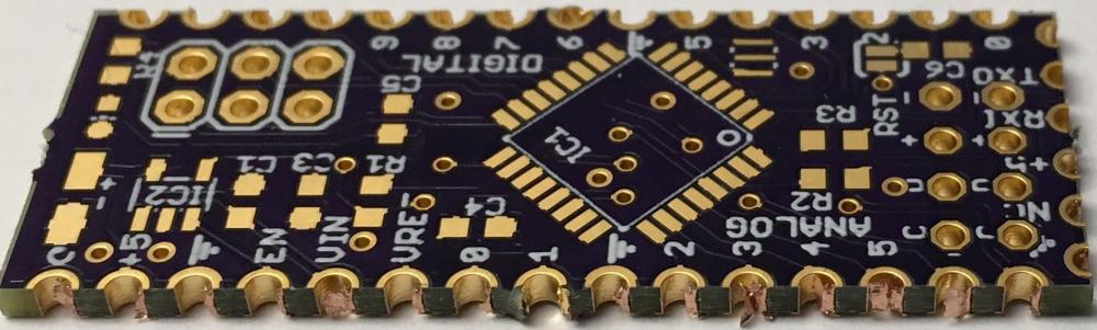
Castellated Mounting Holes
When we make a circuit board, we refer to the mounting holes as castellated. In this type of design, there is the application of two different copper platings. A tin-plated PCB can have a thin layer of copper with a surface coating of anti-corrosion tin. The copper layer inside the castellated holes is then exposed. In addition to providing mechanical stability for the PCB, the copper-plated design eliminates the problems associated with copper skin and twisting.
Unlike other methods of PCB assembly, we can use castellated holes for combining two boards. This feature is especially useful for breakout boards, small modules, and PCB to PCB links. As a result, these PCBs have excellent compatibility and can be useful in various applications. You can also use these holes to make wireless PCB-to-PCB connections. As the name implies, castellated holes can be a great way to combine two boards into one.
There are several requirements for manufacturing castellated holes. The minimum diameter of the hole must be 0.6 mm. The minimum diameter of the holes must be identical to the hole diameter on the board outline/mechanical layer. If there are half holes, choose the “Yes” option and pay the extra fee. This option will require that the holes be at least 0.6 mm in diameter. If you choose “No,” there will be no additional fee for half-holes.
Castellated holes
Pad size is the most important factor when designing and creating castellated holes in PCBs. The most massive pads are best for these PCBs because they make it easier to align components. Moreover, the largest pads are also the best choice for castellated holes because you can drill them easily. This also reduces the risk of component liftoff and contamination during soldering. You can also make your own castellated holes by using the castellated hole features of Altium Designer.
The process of forming castellated holes is different from the traditional one. First, you need to drill the edge of the substrate plate. You will need to use specialized equipment for this step. Then, you should deposit a copper layer into the hole to ensure the excellent conductivity of the components. The whole process takes a few days, so you should make sure you hire a professional. Castellated holes in PCBs are an important part of many electronic devices, and you must ensure that the manufacturers you work with have the right skills and equipment for the job.
To meet the high standards of PCB manufacturing, manufacturers of castellated holes must be compliant with several design attributes. These include ENIG surface finish, large pads, and optimum hole numbers. Meeting these design attributes is essential for a successful end-product, as they can result in a faulty board.
Applications of Castellated holes
One of the most important considerations in PCBs’ manufacturing process is the hole’s size. To achieve the best results, use a minimum hole diameter of 1.0 mm, about 0.04 inches. Ideally, a castellated hole should be on the top or bottom of the board’s edge. Do not place it on the vertical board edge, as it will act as a bridge and hold the PCB in place.
Castellated holes are good for breakout boards in integrated modules in the manufacturing process. The castellated PCBs are capable of replicating specific components on a circuit board. For example, castellated PCBs can be useful to duplicate an inverter, filter, feedback loops, or any other part that requires multiple pins. In this way, castellated PCBs are flexible and can be mass-produced. They are also good as breakout boards, so users can change the pin layout of individual components as needed.
Apart from PCBs, castellated holes also allow the mounting of SMD components. This feature is especially useful for PCB boards with smaller diameters, as they are easier to work with and may not fit the standard PCB fabrication process. However, it is important to comply with the relevant certification standards before purchasing castellated holes. If you fail to do so, you risk getting a faulty board. But with castellated hole PCBs, this issue will not be a problem, as they are a popular choice for smaller PCB modules.
Half holes
In manufacturing a PCB, there is the plating of half holes. The holes must have an electrical connection. A physical connection is not enough – space the holes need with zero spacing between them. Even a small gap will affect soldering. However, plated half holes are not that hard to produce. So, you should be able to find an inexpensive PCB manufacturing company that can provide you with this feature.
To obtain a high-quality plated half-hole PCB, you should know how to recognize them. Half-holes are usually visible on the surface of a PCB, and the hole size is 0.55 mm or 0.06 mm, which is the actual size of two half-hole plates. Generally, a PCB manufacturer will supply you with a sample of these holes to ensure the quality of the board.
A Plated Half Hole PCB from Castellations is a great choice for all of your upcoming PCB projects. You manufacture this PCB with plated half holes, allowing electrical contact between its components. As PCB sizes decrease and geometric index increases, round holes are often insufficient to support the board’s components. Using a plated option, you’ll avoid the problems associated with cold soldering and achieve a superior electrical connection.
PCB Assembly Process
The Castellations PCB assembly process involves the formation of partial holes in the board through which you place electrical contacts. During proper alignment and assembly process, the thickness of the upper PCB is usually one-third the size of the lower one. Stacking can be more complicated if the holes are not parallel. It is therefore essential to stack the boards without creating any gaps. To improve the stacked PCBs, the copper layer on the hole’s wall must be similar to the size of the board’s component pads.
As with any other PCB, the holes of a castellated PCB must match the pads of the components it supports. If this is not possible, plate the holes in a different way and place the second row of through-holes. This way, you can mount the castellated PCB in a production castellated module. The next step is to determine where to locate the holes.
PCB board
A Castellations PCB board is a printed circuit board that uses two copper platings. The first copper plating is an anti-corrosion tin, which has to adhere to the substrate. The tin is removed by peeling off the board’s edge, exposing the copper of the Castellation holes. This process eliminates copper residue, copper skin, and twisting problems. Additionally, it reduces the amount of soldering flux used and can increase the reliability of the PCB.
As the density and functionality of electronic goods have increased, so has the soldering process. Many traditional processes require the soldering of round holes in the motherboard. This process can lead to cold solder, resulting in an inferior electrical connection. Many devices now incorporate plated half holes to ensure the PCB is properly conductive. A PCB with a large hole could cause an electronic product to fail. The Castellations PCB board is the ideal solution for these situations.
Surface Mount PCBs
To create castellated Surface Mount PCBs, it’s necessary to know the proper dimensions of the components and board layout. This way, you can size castellated PCBs to fit the space available. The holes in castellated circuit boards should be the largest possible sizes. If you use smaller holes, it can be difficult to align the components. It’s also important to check the size of the pads on the castellated board.
To make PCBs with castellated vias, you must have copper on the surface of the board and tin on the underlying substrate. For this process, you must indicate the copper through round pads, extending 40 mil from the edge of the board. Peel off the tin on the board, exposing the copper in the Castellation holes. In addition, this process eliminates copper skin and its twisting and curling problems.
The plated half holes on surface mount PCBs help turn them into a surface mount subassembly. These half holes are commonly useful as breakout circuits for fine-pitch SMD components. These holes also provide better soldering landings and eliminate space for dust. Semi-plated half holes are also widely used in microcontroller modules, display PCBs, and breakout PCBs.
The traditional process of using a solder mask and plated through holes on a PCB is no longer sufficient. As the density and multi-functionality of electronic goods increase, it’s vital to change the soldering process. A round hole plated with flux leads to cold solder that is not as good as a plated through hole. Large holes may also damage an electronic product, so plated half holes are becoming increasingly popular.
Breakout Board
In most cases, the breakout board for a bigger PCB will have a plated half-hole. This feature makes it possible to install various Printed Circuit Board modules without creating a void. It is also important for board-to-board connections. This hole style also allows for precision soldering and the development of a single PCB based on integrated modules.
It is important to select the correct surface finish for the castellated PCB. ENIG is the recommended finish for this type of board. The type of finish will depend on the intended application. For example, holes in castellated circuit boards should be the largest sizes available. Depending on the PCB design, it may be difficult to align pads. When choosing the size of holes, the manufacturer of the castellated PCB will make a recommendation for the appropriate number of holes.
Board to board soldering
This method can achieve a high level of reliability, which is necessary for high-reliability applications. However, there are a few things that you should keep in mind before you begin. Board to board soldering for castellations PCB requires that the pads on the main board be large enough to accept the entire solder fillet. Secondly, the solder mask must have a small enough expansion to prevent bridging.
The plated half-hole is an important aspect of the soldering process and needs precise positioning to ensure proper electrical contact. Otherwise, the solder will become weak. Lastly, it is important to avoid cold soldering, as this will result in an unreliable electrical link. A proper soldering process is essential to ensuring a strong, long-lasting connection when soldering a board to a main PCB board.
Castellation PCB and Plated Holes
If you’re in the market for a custom PCB with castellated holes, you’ve likely come across the solder mask opening. These openings occur where solder masks do not cover the copper layers of the board. These are important for castellation PCB users because they can prevent solder bridges between adjacent pads.
Traditional castellation holes are relatively simple to manufacture. Drilling and application of chemical copper are the first two steps. After that, they’re followed by pattern plating or panel plating, stripping the mask, and surface finishing. Afterward, the castellation process and outline milling complete the production process. Aside from assembling the PCBs, castellation PCB and Plated Holes can also be used to manufacture wireless PCB connections.
Placing flux on the surface of the board before soldering is an important step to ensure a quality assembly. Soldering flux on the board can cause flux residue to form. It will be amber, black, or sticky. To clean the board of flux, simply wipe it with rubbing alcohol. Also, using a Kimwipe to avoid lint on the board is recommended. Canned air is a good way to clean the board as well.
Wi-Fi Modules
There are many ways to solder the vias on a Castellations Wi-Fi Modules PCB. Some methods are known as Through Hole Technology (THT) or Surface Mount Technology (SMT). This process involves mounting a board on top of another PCB. Castellations are the links that connect the PCB to the module. You can use either method, depending on your needs. Regardless of your method, you must avoid too much solder to the connections.
Create Wireless PCB
The process of creating a wireless PCB with Castellations is relatively simple. You can treat the holes of the castellated board like through-hole components. The pads of the main board are large enough to accommodate the entire solder fillet, and the holes themselves are small enough to allow for the remaining solder fillet to fill the gap. This makes soldering the boards together easy. Before you begin, however, you should make sure that the pads of your main board are large enough to accommodate the entire fillet.
Start by creating a design that shows all the components and their connections. Then, you need to place the solder mask on the castellated PCB. This will prevent any problems with soldering, such as copper residue twisting. After you have done this, the next step will be to cut and mount the castellated PCB. This is a fairly simple process but can be a little time-consuming.


