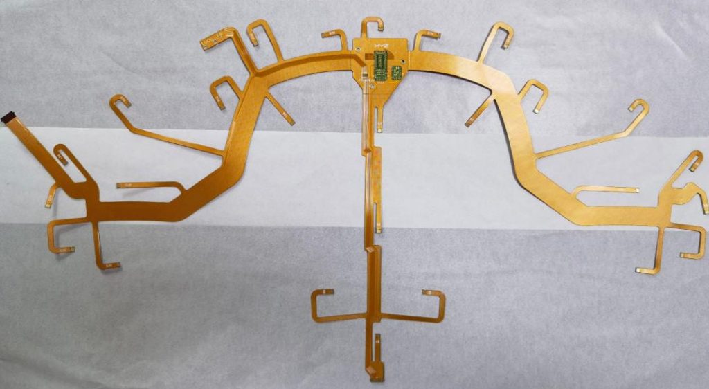
Smaller copper characteristics and some other board materials are used on ultra-thin flex PCBs that are very thin. These devices lack the stiffness of regular circuit boards and are incredibly lightweight.
Demand for ultra-thin flexible PCBs is increasing along with the demand for increasingly more miniature devices. Compact devices for mobile, wearables, implantable, and other tiny devices must be developed with PCBs.
The Benefits of Ultra-Thin Flexible PCBs
In addition to their size, ultra-thin flexible PCBs provide a number of benefits. For your gadget, using a flexible PCB secures a number of advantages:
- Reduce material costs: PCBs contain components of pricey components like copper. Thinner boards have cheaper material costs since they use fewer of those components. This decrease equalizes production and handling costs.
- Compatibility with cutting-edge methods: Ultra-thin PCBs may be used with cutting-edge methods such as direct laser imaging. These methods can be employed with caution and exact registration procedures without causing harm to the flex PCB.
- Dependability: Custom repeating routing pathways can be hosted on an extra-thin circuit board. You’ll experience low service calls because of the greater dependability that each flex board brings.
- Improved defense: These Boards feature polyimide coverings on the conductors. This dielectric layer, along with other cover and base materials, provides defense against a number of potentially dangerous circumstances.
- Low mass and high ductility: These characteristics lessen stress and impact on the solder joints and flex boards. Low mass and excellent ductility assist the flex PCB in tolerating harsh operating circumstances since acceleration and vibration are particularly difficult for such joints.
- Robustness: Ultra-thin Printed Circuit Boards can withstand many flexing cycles. A PCB preserves the integrity of both materials by acting as a transitional element between flexible and stiff sections.
Material For Ultra-Thin Flexible PCBs

A new level of PCB miniaturization is made feasible by thin base substances. While shrinking PCBs in the direction of Z results in a thinner board and more room for components, shrinking circuit boards in the Y and X dimensions just decrease their footprint.
- Copper layers: Flex PCB connections require less plated copper than rigid PCB connectors. The connector footprint is lower because of such thin layers of copper. Moreover, thinner layers produce lines and spaces with little resolution.
- Polyimide: Coatings and layers constructed of polyimide offer additional security without bulking up the electronic circuit.
- Adhesive: To join and attach various bending pieces so they can tolerate flexing, layers of high-quality glue are used.
For small devices like hearing aids and medical implants, flexible ultra-thin substrates are necessary. The size of all these components affects patient comfort because thin substrates flex more easily. Flat substrates have to possess the flexibility to fold and bend without harming the circuit board in order to minimize their size.
Ultra-Thin Flexible PCB Application
Extra-thin PCBs are perfect for uses where it is hard to utilize other types of PCBs. Designers often choose a flexible PCB because of its distinct benefits over wires and conventional PCB design. Flex PCBs may be bent to fit any area or package while exhibiting the same uniformity, density, and accuracy as rigid PCBs.
Flex circuits are found in drawing boards, SIM cards, metro coins, and implantable and wearable medical devices.
Replace wiring harnesses with flex circuits for one of their most popular uses. Many hardboards, wires, and connections can be replaced with a single flex PCB.
By eliminating the need to color-code and bundle wires during assembly, applying these kinds of boards can save both labor and supplies. There are three significant benefits to streamlining this procedure:
Faster production rates, lower installation expenses, and fewer assembly- and service-related issues
A flex board can take the place of wire harnesses to increase the repeatability of wiring routing, and by removing mistakes, test durations, repairs, and rejections are reduced. Moreover, flat strip conductors may carry a greater current than circular wires and are better at dissipating heat. Stronger relationships are produced by these traits. A designer has more control over impedance, noise, and crosstalk after they decide on a consistent conductor arrangement for the flexible PCB.
Types Of Ultra-Thin PCBs

Two main varieties of long, thin Printed Circuit Boards are available. These are ultra-thin flex PCB and rigid PCB.
· Rigid Ultra-Thin PCB:
For applications that need a 2D PCB, stiff ultra-thin PCB materials are readily available. Typically, you may use them as a substrate for packing ICs, or integrated circuits. Here, they assist in making the component as a whole incredibly thin.
You may find 25-micron lines as well as broad gaps, 175-micron or smaller pitches, and 50 and 100-micron vias and pads here.
· Ultra-Thin Flexible PCB:
Also known as super thin flexible PCB. Often, flexible laminates are used to create this long, thin Board. The PCB might collapse as a result. As a result, less space is needed to store or encapsulate the board on both a surface area and volume level. The density of integration rises as a result.
Additionally, superior bending is made simple by the ultra-thin Circuit. The manufacture of cables that need dynamic bending is one use for ultra-thin flex PCBs. This is a result of their strong bending abilities.
Single-Sided Ultra-Thin PCB Vs. Double-Sided Ultra-Thin PCB: What’s The Difference?
Conducive copper is used on the single-layered, ultra-thin Circuit, and components are put on each of the sides of the board. It also features conductive wire on the opposite surface. This is the only kind of long, thin PCB that is commonly manufactured. This is due to their fundamental character and simplicity.
Single-layered PCBs are frequently used in a variety of devices, such as radio equipment, printers, calculators, camera systems, and more.
Contrarily, double-layered ultra-thin Circuits have traces on both sides with a bottom and top layer. Any surface of the board may be simply fitted with active copper and electrical components. This makes it possible for the traces to pass through one another. The end product is high-density circuitry that doesn’t require soldering.
The fabrication of double-sided extremely thin PCBs may be more difficult since they are more complex than their single-sided equivalents. Nonetheless, the advantages of double-layered, ultra-thin PCBs outweigh their drawbacks by a wide margin.
The most popular variety of double-layered ultra-thin PCBs is the latter. This is so that highly complex boards may be produced with their assistance. This is advantageous for PCB purposes as well as devices involving advanced electronics.
Double-layered long thin Circuits are used in a variety of devices, including vending machines, lighting systems, amplifiers, and automotive dashboards.
Drill Microvias Into Ultra-Thin PCB
For drilling micro vias onto extremely thin PCBs, there are many methods that exist. They consist of plasma etching, laser drilling, and photo-via drilling. Let’s examine each of these methods in turn.
· Photo-via Drilling:
Photo-imaginable dielectric material and lithographic patterning are used in photo-via equipment. The development of the ultra-thin HDI Circuit has been made possible by this technology. Additionally, the hole’s size is around 25 m in both depth and diameter. Also, the dielectric substance used in this drilling technique makes it pricey.
· Plasma Etching:
Using plasma, this micro via-drilling technique etches the PCB material to create holes. With this method, it is possible to create a via house with a 75 mm diameter out of substances that are about 25 mm thick.
Yet, this approach is the least expensive for digging the via compared to other expenditures associated with vacuum equipment.
· Laser Drilling:
The most intriguing of all is this drilling technique. For dielectric materials with a thickness of 5 m, you may use this approach to increase the diameter of the vias up to 5 m.
The wavelength, thickness of substrate material, substrate type, and density of energy are the main driving forces behind such a micro via drilling process.
The best technique for micro vias, typically involving concentrating the laser light on an extremely small region, is this one. The vias that are produced are equally as clean as those made by mechanical drilling. By doing this, it is ensured that the plating is applied uniformly to the inside of the vias.
In contrast to mechanical drilling, this approach has a slower drill speed. Using any wavelength between ultraviolet and far-infrared, you may use this technology to easily drill the thick micro vias inside an ultra-thin Circuit.
However, this method has a drawback. This is due to the laser beam’s restricted depth, which can be drilled with consistency and dependability. The maximum depth a laser can dig is constrained when just one lens is used for beam concentration. This is a result of the limited depth of focus.
Yet, a collimated laser beam guarantees that the laser, via the form of drilling, reaches a significantly greater depth. The via’s extremely small size, which results in the Fresnel diffraction of the beam, is a problem in this case. This, in turn, may have an effect on the beam’s intensity in extremely deep micro via holes.
Conclusion
We believe we have covered all the necessary information regarding ultra-thin Printed Circuit Boards. As has been mentioned, this form of PCB is thinner than the normal one. Moreover, it provides less weight and is more compact. This is a result of the board’s materials being used less.
Many PCB manufacturers provide you with the finest by providing you with customized ultra-thin Circuits based on what your particular demands are. For affordable rates and high-performance solutions for the ultra-thin PCB, contact RayPCB now.


